Sharp SD-EX101 Service Manual - Page 74
ICD02 RH-iX0526AWZZ: System Microcomputer IX0526AW [To Serial No. 20x04000] 1/3
 |
View all Sharp SD-EX101 manuals
Add to My Manuals
Save this manual to your list of manuals |
Page 74 highlights
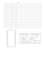
SD-EX100 SD-EX101 ICD02 RH-iX0526AWZZ: System Microcomputer (IX0526AW) [To Serial No. 20x04000] (1/3) ICD02 RH-iX0567AWZZ: System Microcomputer (IX0567AW) [From Serial No. 20x04001] (1/3) Pin No. Port Name Terminal Name Input/Output Function 1 P96/ANEX1/SOUT4 FLD_SDATA Output Display data output to FL driver M66005 2 P95/ANEX0/CLK4 FLD_SCK Output Serial clock output to FL driver M66005 3 P94/DA1/TB4IN TRY_M+ (D/A) Output CD Tray OPEN/CLOSE control motor normal rotation control output D/A output (Three-valued output) 4 P93/DA0/TB3IN TRY_M- (D/A) Output CD Tray OPEN/CLOSE control motor inversion control output D/A output (Three-valued output) 5 P92/TB2IN/SOUT3 FLD_CS Output Chip select output to FL driver M66005 6* P91/TB1IN/SIN3 Output Port processing. Fixed at "L". 7* P90/TB0IN/CLK3 Output Port processing. Fixed at "L". 8 BYTE BYTE Input External bus unused; connected to VSS 9 CNVSS FLASH_VCC Input Used in single chip mode. Connected to VSS via pull-down resistor In case of Flash writing: VCC exclusively for exterior 10 P87/XCIN XCIN Input Crystal for clock 32,768 kHz connected 11 P86/XCOUT XCOUT Output Crystal for clock 32,768 kHz connected 12 RESET RESET Input Reset input for the microcomputer. Active: "L". In case of Flash writing: Connect to RESET 13 XOUT X_OUT Output Reference oscillation output for the microcomputer 8.4 MHz CERALOCK connected 14 VSS VSS - Connected to GND (VSS) 15 XIN X_IN Input Reference oscillation output for the microcomputer 8.4 MHz CERALOCK connection 16 VCC VCC Input Power supply to the microcomputer (3.3V) Backup power supply 17 P85/NMI NMI Input Connected to VCC via pull-up resistor (Setting in case of FLASH writing) Functionally unused. 18 P84/INT2 P_IN Input Power failure detection input Power failure detected according to detection time "H" "L". 19* P83/INT1 - Output Port processing. Fixed at "L". 20 P82/INT0 RX_IN Input Remote control input by SHARP system 21* P81/TA4IN/U - Output Port processing. Fixed at "L". 22* P80/TA4OUT/U - Output Port processing. Fixed at "L". 23* P77/TA3IN - Output Port processing. Fixed at "L". 24* P76/TA3OUT - Output Port processing. Fixed at "L". 25* P75/TA2IN/W - Output Port processing. Fixed at "L". 26 P74/TA2OUT/W P_DOWN Output "H" for power ON. "L" for power failure. 27* P73/CTS2/RTS2/TA1IN/V - Output Port processing. Fixed at "L". 28* P72/CLK2/TA1OUT/V - Output Port processing. Fixed at "L". 29* P71/RXD2/SCL/TA0IN/TB5IN - Output Port processing. Fixed at "L". 30* P70/TXD2/SDA/TA0OUT - Output Port processing. Fixed at "L". 31 P67/TXD1 (MD)K_DATA FLASHTXD Output K Data output serial 32 bytes. Automatic reception/transmission (Transmission data output to FLASH writer) 32 P66/RXD1 (MD)MD_DATA FLASHRXD Input MD Data input serial 32 bytes. Automatic reception/transmission (Transmission data output to FLASH writer) 33 P65/CLK1 (MD)DSCK/ FLASHSCLK Output MD Clock output serial 32 bytes. Automatic reception/transmission (Transmission data output to FLASH writer) 34 P64/CTS1/RTS1/CTS0/CLKS1 (MD)D_STB/ Input MD_STB Input. For transmission control FLASHBUSY (Transmission data output to FLASH writer) 35 P63/TXD0 - Output Port processing. Fixed at "L". 36 P62/RXD0 - Output Port processing. Fixed at "L". In this unit, the terminal with asterisk mark (*) is open terminal which is not connected to the outside. - 74 -
-
 1
1 -
2
-
3
-
4
-
5
-
6
-
7
-
8
-
9
-
10
-
11
-
12
-
13
-
14
-
15
-
16
-
17
-
18
-
19
-
20
-
21
-
22
-
23
-
24
-
25
-
26
-
27
-
28
-
29
-
30
-
31
-
32
-
33
-
34
-
35
-
36
-
37
-
38
-
39
-
40
-
41
-
42
-
43
-
44
-
45
-
46
-
47
-
48
-
49
-
50
-
51
-
52
-
53
-
54
-
55
-
56
-
57
-
58
-
59
-
60
-
61
-
62
-
63
-
64
-
65
-
66
-
67
-
68
-
 69
69 -
 70
70 -
 71
71 -
 72
72 -
 73
73 -
 74
74 -
 75
75 -
 76
76 -
 77
77 -
 78
78 -
 79
79 -
80
-
81
-
82
-
83
-
84
-
85
-
86
-
87
-
88
-
89
-
90
-
91
-
92
-
93
-
94
-
95
-
96
-
97
-
98
-
99
-
100
 |
 |