Sharp SD-EX101 Service Manual - Page 73
IC900 VHiPCM1748E-1: D/A Converter PCM1748E
 |
View all Sharp SD-EX101 manuals
Add to My Manuals
Save this manual to your list of manuals |
Page 73 highlights
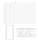
IC900 VHiPCM1748E-1: D/A Converter (PCM1748E) Pin No. 1 2 3 4 5 6 7 8 9 10 11* 12* 13 14 15 16 Terminal Name BCK DATA LRCK DGND VDD VCC VOUTL VOUTR AGND VCOM ZEROR/ZEROA ZEROL/NA MD MC ML SCK Input/ Output Input Input Input - - - Output Output - - Output Output Input Input Input Input Function Audio data bit clock input. Audio data digital input. L-channel and R-channel audio data latch enable input. Digital ground. Digital power supply,+3.3V. Analog power supply,+5V. Analog output for L-channel. Analog output for R-channel. Analog ground. Common voltage decoupling. Zero flag output for R-channel/Zero flag output for L/R-channel. Zero flag output for L-channel/No assign. Mode control data input. Mode control clock input. Mode control latch input. System clock input NOTE: (1) Schmitt trigger input,5V tolerant. (2) Schmitt trigger input with internal pull-down,5V tolerant In this unit, the terminal with asterisk mark (*) is open terminal which is not connected to the outside. SD-EX100 SD-EX101 (1) (1) (1) (2) (2) (2) AGND 9 VCOM 10 6 VCC ZEROR/ZEROA 11 5 VDD ZEROL/NA 12 MD 13 MC 14 ML 15 SCK 16 8 VOUTR 7 VOUTL 4 DGND 3 LRCK 2 DATA 1 BCK BCK 1 LRCK 3 DATA 2 Audio Serial Port ML 15 MC 14 MDI 13 Serial Control Port 8x Oversampling Digital Filter with Function Controller Enhanced Multi-level Delta-Sigma Modulator SCK 16 System Clock System Clock Manager Zero Detect 12 11 DAC Output Amp. and Low-pass Filter DAC Output Amp. and Low-pass Filter Power Supply 54 69 7 VOUTL 10 VCOM 8 VOUTR ZEROL ZEROR VDD DGND VCC AGND Figure 73 BLOCK DIAGRAM OF IC - 73 -
-
 1
1 -
2
-
3
-
4
-
5
-
6
-
7
-
8
-
9
-
10
-
11
-
12
-
13
-
14
-
15
-
16
-
17
-
18
-
19
-
20
-
21
-
22
-
23
-
24
-
25
-
26
-
27
-
28
-
29
-
30
-
31
-
32
-
33
-
34
-
35
-
36
-
37
-
38
-
39
-
40
-
41
-
42
-
43
-
44
-
45
-
46
-
47
-
48
-
49
-
50
-
51
-
52
-
53
-
54
-
55
-
56
-
57
-
58
-
59
-
60
-
61
-
62
-
63
-
64
-
65
-
66
-
67
-
 68
68 -
 69
69 -
 70
70 -
 71
71 -
 72
72 -
 73
73 -
 74
74 -
 75
75 -
 76
76 -
 77
77 -
 78
78 -
79
-
80
-
81
-
82
-
83
-
84
-
85
-
86
-
87
-
88
-
89
-
90
-
91
-
92
-
93
-
94
-
95
-
96
-
97
-
98
-
99
-
100
 |
 |
