Acer Altos T110 F4 Service Guide - Page 8
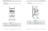
C232 Chipset Block, Diagram
 |
View all Acer Altos T110 F4 manuals
Add to My Manuals
Save this manual to your list of manuals |
Page 8 highlights
SuperWorkstation 5039D-I User's Manual Connector PCI-E (PCH) Slot 5 SP1 USB 0/1 USB 2/3, USB 4/5 USB 6/7 USB 8/9 USB 10 VGA Description PCI-Express 3.0 x4 in x8 Slot Internal Speaker/Buzzer Back Panel USB 2.0 Ports Front Accessible USB 2.0 Headers Back Panel USB 3.0 Ports Front Accessible USB 3.0 Header USB 3.0 Type-A Header VGA Port 14 Chapter 1: Introduction PCIe3.0 x8 (in x8) PCIe3.0 x8 (in x16) PCI-E X8 Gen3 PCI-E X8 Gen3 IMVP 8 3 PHASE for Vcore 80W #8-15 #0-7 Skt-H4 LGA1151 DMI3 RJ45 RJ45 LAN1 I210 LAN2 I210 PCI-E X1 Gen3 #9 PCI-E X1 Gen3 #10 DMI3 x4 #1/2/3/4 #5/6/7/8 DDR4 2133 DDR4 2133 #A-2 #A-1 #B-2 #B-1 PCI-E x4 Gen3 PCIe3.0 x4 (in x8) PCI-E x4 Gen3 PCIe 3.0 x4 (in x8) RMII/NCSI SATA RJ45 LAN3 RGRMII RTL8211E-VB-CG DDR3 SPI BMC Boot Flash BMC AST2400 PCI-E X1 Gen1 #11 USB 2.0 #9 SPI PCH 6.0 Gb/S USB 3.0 USB3.0 USB2.0 VGA CONN COM1 COM2 Connector Header Temp Sensor EMC1402-1 *2 at diff SMBUS SYSTEM POWER FAN SPEED CTRL FRONT PANEL SPI MUX SPI BIOS USB 2.0 LPC TPM Header Debug Card Figure 1-5. C232 Chipset Block Diagram Note: This is a general block diagram and may not exactly represent the features on your motherboard. Note the differences marked between the X11SSL-F (included in the T110 F4) and the X11SSM. See the Appendix C for the actual specifications of your motherboard. 15
-
 1
1 -
2
-
 3
3 -
 4
4 -
 5
5 -
 6
6 -
 7
7 -
 8
8 -
 9
9 -
 10
10 -
 11
11 -
 12
12 -
 13
13 -
14
-
15
-
16
-
17
-
18
-
19
-
20
-
21
-
22
-
23
-
24
-
25
-
26
-
27
-
28
-
29
-
30
-
31
-
32
-
33
-
34
-
35
-
36
-
37
-
38
-
39
-
40
-
41
-
42
-
43
-
44
-
45
-
46
-
47
-
48
-
49
-
50
-
51
-
52
-
53
-
54
-
55
-
56
-
57
-
58
-
59
-
60
 |
 |
