ViewSonic VE710S Service Manual - Page 13
Circuit Description - monitor
 |
UPC - 766907153941
View all ViewSonic VE710S manuals
Add to My Manuals
Save this manual to your list of manuals |
Page 13 highlights
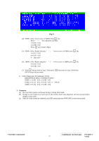
4. Circuit Description A. Scaling controller The ADC converts RGB analog signals to digital signals that the scaling chip can acknowledge. The HSYNC input receives a logic signal and provides the frequency reference for pixel clock generation. The scaling IC converts the input signal ranging from VGA to SXGA into SXGA resolution that panel can acknowledge. GENERAL DESCRIPTION The MST8116A is a high performance, and fully integrated graphics processing IC solution for LCD monitors with resolutions up to SXGA. It is configured with an integrated triple-ADC/PLL, a high quality scaling engine, an on-screen display controller, a built-in output clock generator, a panel timing controller (TCON), and RSDS display interface. To further reduce system costs, the MST8116A also integrates intelligent power management control capability for green-mode requirements and spread-spectrum support for EMI management. PIN DESCRIPTION CPU Interface Pin Name Pin Type Function Pin HWRESET Schmitt Trigger Input w/ 5V-tolerant Hardware reset; active high 32 CS Input w/ 5V-tolerant 3 Wire Serial Bus Chip Select; active high 69 SDA I/O w/ 5V-tolerant 3 Wire Serial Bus Data; 4mA driving strength 70 SCL Input w/ 5V-tolerant 3 Wire Serial Bus Clock 71 INT Output CPU interrupt; 4mA driving strength 72 Analog Interface Pin Name Pin Type Function Pin HSYNC0 Schmitt Trigger Input w/ 5V-tolerant Analog HSYNC input 37 VSYNC0 Schmitt Trigger Input w/ 5V-tolerant Analog VSYNC input 38 REFP Internal ADC top de-coupling pin 66 REFM Internal ADC bottom de-coupling pin 67 RIN0 Analog Input Analog red input 63 RIN0M Analog Input Reference ground for analog red input 62 SOGIN0 Analog Input Sync-on-green input 61 GIN0 Analog Input Analog green input 60 GIN0M Analog Input Reference ground for analog green input 59 BIN0 Analog Input Analog blue input 58 BIN0M Analog Input Reference ground for analog blue input 57 REXT External resistor 390 ohm to AVDD 52 RSDS Interface Pin Name Pin Type Function Pin CLKAP Output A-Link Positive RSDS Differential Clock Output from"Odd" Channel 118 ViewSonic Corporation Confidential - Do Not Copy VE710s/b-2 10 VA721
-
 1
1 -
2
-
3
-
4
-
5
-
6
-
7
-
 8
8 -
 9
9 -
 10
10 -
 11
11 -
 12
12 -
 13
13 -
 14
14 -
 15
15 -
 16
16 -
 17
17 -
 18
18 -
19
-
20
-
21
-
22
-
23
-
24
-
25
-
26
-
27
-
28
-
29
-
30
-
31
-
32
-
33
-
34
-
35
-
36
-
37
-
38
-
39
-
40
-
41
-
42
-
43
-
44
-
45
-
46
-
47
-
48
-
49
-
50
-
51
-
52
 |
 |
