Kenwood TK-3101K Service Manual - Page 8
Transmitter
 |
View all Kenwood TK-3101K manuals
Add to My Manuals
Save this manual to your list of manuals |
Page 8 highlights
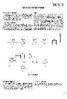
TK-3101 CIRCUIT DESCRIPTION PLL DATA PLL IC ICI 5kHz/6.25kHz UN LPF REF OSC PHASE COMPARATOR CHARGE PUMP I/M 5kHzI6.25kHz D2, 4 O4 TX VCO Dl, 3 O3 RX VCO O2 RF AMP O6 BUFF AMP O5, 7 T/R SW 12.8MHz T Fig. 4 PLL circuit 3) UNLOCK DETECTOR 5C If a pulse signal appears at the LD pin of IC1, an unlock condition occurs, and the DC voltage, obtained from D7, R6, and IC1 C1 causes the voltage applied to the UL pin of the R6 D7 IC403 microprocessor to go low. When the microprocessor detects this LD UL condition, the transmitter is disabled, ignoring the push-to-talk switch input signal. ( See Fig.5) PLL IC I CI MPU Fig. 5 Unlock detector circuit 4. Transmitter 1) Transmit audio The modulation signal from the microphone is amplified by IC500 (1/2), passes through a preemphasis circuit, and amplified by the other IC500 (1/2) to perform IDC operation. The signal then passes through a low-pass filter (splatter filter) (Q501 and Q502) and cuts 3kHz and higher frequencies. The resulting signal goes to the VCO through the VCO modulation terminal for direct FM modulation. (See Fig. 6) 2) OT/DOT encoder A necessary signal for QT/DQT encoding is generated by IC403 and FM-modulated to the PLL reference signal. Since the reference OSC does not modulate the loop characteristic frequency or higher, modulation is performed at the VCO side by adjusting the balance. (See Fig. 6) IC500 (1/2) MIC AMP PREEMPHASIS IC500 (1/2) IDC O501, 502 LPF (SPLATTER FILTER) VR501 MAX DEV MIC D5, O4 VCO O503 SW IC403 OT/DOT TO MUTE Fig. 6 Transmit audio QT/DOT VR500 BALANCE X1, IC1 REFERENCE OSC (TCXO) 8
-
 1
1 -
2
-
 3
3 -
 4
4 -
 5
5 -
 6
6 -
 7
7 -
 8
8 -
 9
9 -
 10
10 -
 11
11 -
 12
12 -
 13
13 -
14
-
15
-
16
-
17
-
18
-
19
-
20
-
21
-
22
-
23
-
24
-
25
-
26
-
27
-
28
-
29
-
30
-
31
-
32
 |
 |
